描述
APPLICATIONS
SUMMARTY
描述
Since the 1950s, the application of semiconductor technology has greatly accelerated the development speed and quality of human civilization. Semiconductor materials have experienced the development and maturity of the application technology of the first and second generation semiconductors, and the third generation semiconductor materials with wide band gap performance are also developing rapidly.
描述
The picture frome Julissa GreenPress. Detailed Introduction to the Third Generation of Semiconductor Materials.
APPLICATIONS
描述
SENSOR
传感器
Automotive Industry
CPU /GPU
Memory Industry
Various acoustic sensors
Various acoustic sensors, attitude sensors, pressure sensors, etc. represented by MEMS sensors are essential core components for various medical equipment, transportation tools, communication equipment, and even aerospace and defense equipment. 
Unlike traditional ICs with a closed protective layer, MEMS is equiped with an extremely fine micro-machining structure. There are very precise fishing lines, gears, hinges, bridges and diaphragm structures inside, and the physical structure is usually very fragile. 

The traditional blade is a water cutting method. Various pollution, vibration, heat and ESD (static electricity) during the cutting process may greatly reduce the performance of MEMS products, and even lead to catastrophic failures of product scrap

Stealth laser cutting is the best solution for MEMS wafer separation

Laser invisible cutting can overcome various technical risks of traditional blade cutting and surface laser cutting due to its inherent technical advantages. The use of laser invisible cutting can minimize various technical risks in the wafer cutting process. Provide the best technical guarantee for the stable mass production of MEMS products.

描述
Another sensors
描述
APPLICATIONS
描述
Automotive Industry 
In the 21st century, the rate of electrification (EV) of automobiles is rapidly expanding. Hybrid vehicles, plug-in hybrid vehicles, pure electric vehicles and even fuel cell vehicles are taking up an increasing market share. The year 2035 is designated by countries all over the world as the first year of the end of fuel vehicle manufacturing. Power electronic technology provides reliable high-voltage, high-current, and high-power power control system protection, which determines the performance and safety of electric vehicles.
Memory Industry
CPU /GPU
Sensor
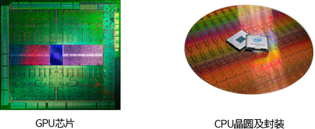
About 10% of the electrical energy is lost due to heat during the power conversion process of traditional power electronic devices. The third-generation semiconductor material silicon carbide (SiC) will greatly reduce the surface resistance (RonA) of electronic components and significantly reduce the through loss.
At present, SiC devices are widely used in power control units (PCU), inverters, DC-DC converters, on-board chargers, etc. of new energy vehicles. With the rapid development and popularization of new energy vehicles, the continues growth of SiC power devices will be driven.
汽车
New energy vehicle power control chip (Sic, GaN) applications include:
描述
APPLICATIONS
描述
CPU / GPU
Stealth laser dicing technology is also the best choice for traditional silicon (Si) chip industry.
After a long history of development, the precision machining technology and circuit forming technology of silicon-based semiconductor have almost reached the limit of material properties. In order to improve the operation speed, the chip itself is also developing to micro refinement and three-dimensional. Image processing chip (GPU) and central processing unit (CPU) with complex integrated computing capability are typical representative products. Their complexity represents the forefront of human semiconductor industry.

 GPU / CPU is characterized with complex structure, large size and high product value. Silicon based semiconductor material is still the main material, and the size of wafer is also developing from 300 mm to 450 mm. The substitution process of the third generation semiconductor materials is also affected by the process maturity and manufacturing cost. At present, it can not replace silicon-based semiconductor materials. For a long time, silicon-based semiconductor wafers have been diced by the mechanical dicing method of diamond hob. This method requires a large amount of pure water for cooling and carbon dioxide injection to generate DI water to eliminate electrostatic hazards. The waste water after dicing requires to be treated. Compared with blade dicing, the dicing path of laser stealth dicing is narrow. The chip output of single wafer is higher and no need of water and other consumables.

Stealth laser dicing technology is the best choice for the highly complex, three-dimensional process of new GPU and CPU industry.
Sensor
Automotive Industry
Memory Industry
CPU
描述
CPU chip
CPU wafer and package
APPLICATIONS
描述
Memory Industry
At present, the memory based on silicon (SI) and semiconductor materials is mostly diced by blade. However, with the global market demand trend of "thinner" and "smaller" semiconductor products, the demand for thinner wafers and smaller devices is growing day by day. Traditional blade dicing has been unable to meet the dicing demand of ultra-thin wafers.
内存
Sensor
Automotive Industry
CPU/GPU
描述
·Process characteristics
Traditional memory wafer dicing technology mainly depends on the combination of blade and laser dicing, which is applied to single complex stack. Due to the different density of material stack structure inside the memory, the use of blade dicing will lead to a very high risk of delamination. Even using laser slotting and blade dicing process, it is difficult to safely dice thin wafers below 50 μM.
·Best solution
Because the laser modification focus can be freely controlled in the depth direction of the wafer, the dicing depth and thickness can be accurately controlled, and the deterministic dicing such as single focus, double focus, multi focus and even full dicing can be realized. The application of general intelligent laser stealth dicing technology is promoting the rapid upgrading of processing technology in memory industry.