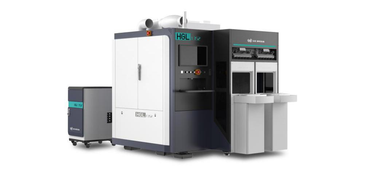
Cutting equipment 1: 20201228: 22233688
SDBG process equipment
描述
HGL Series
Introduction of SDBG equipment (process introduction)
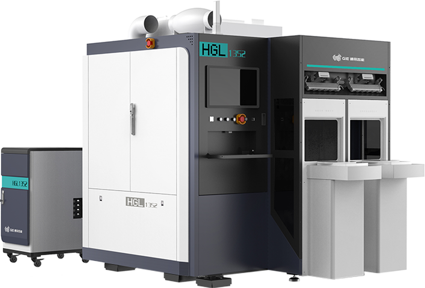
HGL1352 series stealth laser cutting equipment is the first SDBG equipment with mass production capacity and approved by advanced packaging enterprises in China. It is an indispensable equipment for processing internal hidden cracks in wafer substrates with high precision in the SDBG process of semiconductor advanced packaging. Integrated the company's core laser technology and a series of advanced technology know-how, in the core technology has made a number of major breakthroughs. The product adopts self-developed high-performance laser and optical system using excellent scattering control technology to ensure the precision of hidden crack induced ultra-high precision air-floating high-speed platform using Load port+6 axis manipulator for real-time compensation and real-time deviation correction in the process of loading / unloading and wafer handling and cutting. HGL1352 series stealth laser cutting equipment can accurately modify the inside of the wafer substrate and induce high-quality internal hidden cracks (BHC) to ensure the quality and reliability of the subsequent wafer thinning and segmentation process, especially suitable for advanced storage, 3D advanced packaging and other ultra-thin chip manufacturing industry, can fully replace imported SDBG equipment.
Separation line
Single focus wafer laser stealth cutting equipment
Suitable for wafers
4 inches to 8 inches
Wafer thickness
3 μ m ~ 1000 μ m
Number of focus
1
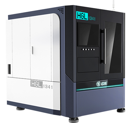
HGL1341 series
Large size single focus wafer laser stealth cutting equipment
Suitable for wafers
4 inches to 12 inches
Wafer thickness
3 μ m ~ 1000 μ m
Number of focus
1
HGL1351 series
Cutting equipment
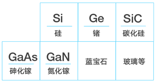
Suitable material
Device-element
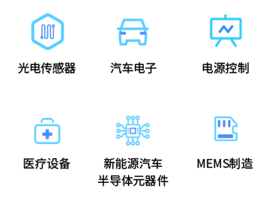
Applied industry
Applied industry
Button 1 "20201229" 101618374
Arrowhead
Single focus stealth cutting equipment
Multi-focus wafer laser stealth cutting equipment
Suitable for wafers
4 inches to 8 inches
Wafer thickness
3 μ m ~ 1000 μ m
Number of focus
1.2.3.4
HGL3341 series
Multi-focus large size wafer laser stealth cutting equipment
Suitable for wafers
4 inches to 12 inches
Wafer thickness
3 μ m ~ 1000 μ m
Number of focus
1.2.3.4
HGL3351 series
Cutting equipment
Suitable material
Device-element
Applied industry
Applied industry
Button 1 "20201229" 101618374
Arrow 3
Multi-focus stealth cutting equipment
Double-focus large-size wafer laser stealth cutting equipment
Suitable for wafers
4 inches to 12 inches
Wafer thickness
3 μ m ~ 1000 μ m
Number of focus
HGL2351 series
2
Cutting equipment
Suitable material
Device-element
Applied industry
Applied industry
Button 1 "20201229" 101618374
Arrow 2
Bifocal stealth cutting equipment
Appearance
Separation line
描述
Performance
Separation line
HGL1352 stealth laser cutting equipment is a domestic high-performance stealth laser cutting equipment independently developed and designed for advanced process semiconductor packaging products represented by solid-state memory.

Equipment modelHGL1352
Optical path sourceIndependent design
Laser sourceChina
Laser cooling modeWater cooling
Laser quality assurance24000 hours
Maximum laser power>18W (@100KHz)
Maximum machined wafer size12 in.
Effective stroke of cutting shaft310mm
Maximum speed of cutting shaft1000mm/s
Maximum acceleration of cutting shaft1.5G
Straightness of cutting axis1um
Effective stroke of Index axis310mm
IndexAxis positioning accuracy±1um
Z-Axis repetitive positioning accuracy1 μ m
Maximum rotation angle of theta axis120 °
Flatness of cutting carrier≤ 5 μ m
Platform pedestalMarble
Cutting platform (X/YAxis)Air-floating high-speed platform
Wafer NotchRecognition modeCalibrator
AFDynamic compensationSupport
AFAltimetry modeSide axle
Beam shapingSLM
High/Low magnification image recognitionIR Camera
Image automatic deviation correction functionSupport

Equipment modelHGL1352
Optical path sourceIndependent design
Laser sourceChina
Laser cooling modeWater cooling
Laser quality assurance24000 hours
Maximum laser power>18W (@100KHz)
Maximum machined wafer size12 in.
Effective stroke of cutting shaft310mm
Maximum speed of cutting shaft1000mm/s
Maximum acceleration of cutting shaft1.5G
Straightness of cutting axis1um
Effective stroke of Index axis310mm
Positioning accuracy of Index axis±1um
Repeated positioning accuracy of Z-axis1 μ m
Maximum rotation angle of theta axis120 °
Flatness of cutting carrier≤ 5 μ m
Platform pedestalMarble
Cutting platform (XUnix Y axis)Air-floating high-speed platform
Wafer Notch recognition modeCalibrator
AF dynamic compensationSupport
AF altimetry modeSide axle
Beam shapingSLM
High / low magnification image recognitionIR Camera
Image automatic deviation correction functionSupport
Application
Separation line
The technological process undertaken by SDBG equipment is an indispensable "high-precision wafer substrate internal hidden crack induction processing" process in the semiconductor advanced packaging industry, and it is one of the most important core equipment in the semiconductor 3D advanced packaging industry. The "2.5D package" and "3D package" integration technology of advanced semiconductor chips around the world is the most important means to improve the performance (speed), power efficiency and cost efficiency of IC. Its representative packaging forms are PBGA, FC-PBGA, 3D BGA,3D integrated chip stack and so on.
Know wealth
Separation line
描述
SDBG is the abbreviation of Stealth Dicing Before Grinding. The SDBG process is different from the traditional wafer cutting process. Before [wafer thinning], high-precision [internal hidden cracks] are induced by invisible laser inside the wafer, and then the wafer is thinned and polished, so that when the wafer is thinned to the thickness that needs to be retained, the stress of grinding and polishing can properly promote the directional propagation of internal hidden cracks. The independent chips on the wafer are naturally separated to obtain high-quality ultra-thin chips (such as the image above). The advantage of SDBG process is not only efficient and safe, but also can make the chip stronger (because SDBG uses the grinding and polishing stage to separate the wafer naturally, it can completely release the internal stress of the wafer caused by cutting, and there will not be quality risks such as "edge collapse" and "cracking" which cannot be avoided by traditional cutting. The ultra-thin chip obtained by SDBG process It is the most advanced, safest and most efficient ultra-thin wafer segmentation technology in the world. The advanced nature and technical advantage of SDBG technology is that it needs to be combined with system engineering such as advanced stealth laser technology, a variety of complex equipment manufacturing technology, advanced control technology and other system engineering to ensure its process effect. The key core technologies are: 1. How to accurately control the scattering of invisible laser inside the wafer substrate and form a modified layer uniformly and stably to accurately induce the development to the front of the wafer with the circuit layer and reach the positive surface of the wafer exactly. At this time, the wafer cannot split. 2. Accurately control the depth of the laser modification layer inside the substrate, so that the modification layer can not reach the range of the chip thickness that needs to be retained (20 ~ 100 μ m). 3. How to control the stress intensity and direction of internal modification to ensure the straightness and verticality quality of hidden cracks. Based on the above technical bottleneck, SDBG process equipment has been monopolized by international equipment manufacturers for a long time, and it is a domestic technology blank equipment.
More Devic